Context & Engineering Objective
High-power AI and high-performance-computing packages combine materials with very different coefficients of thermal expansion. During fabrication cool-down and service thermal cycling, the PCB, glass core, silicon dies, copper, underfill, and SAC305 solder all try to expand by different amounts. The resulting constraint can warp the package and accumulate inelastic strain at solder-pad and intermetallic interfaces.
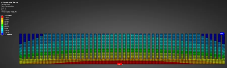
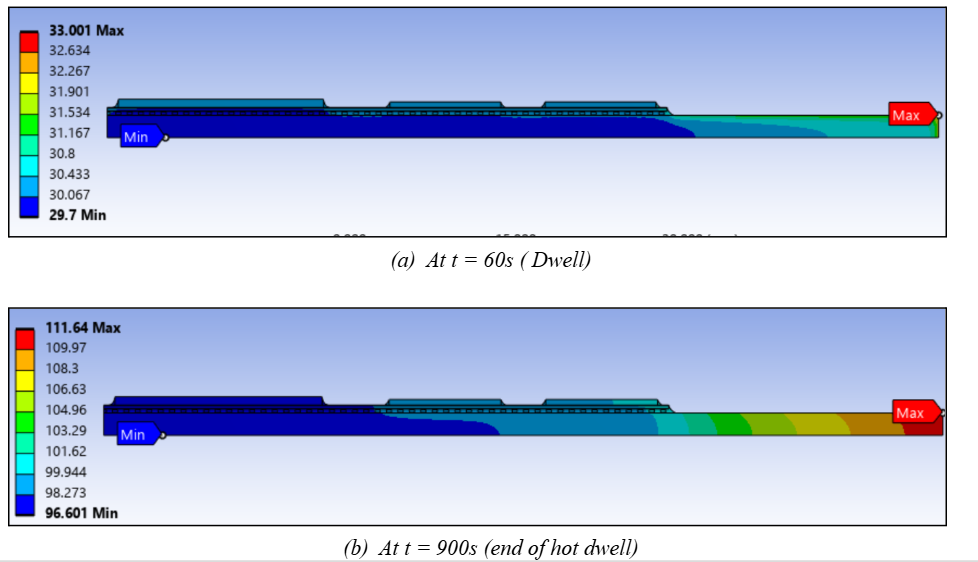
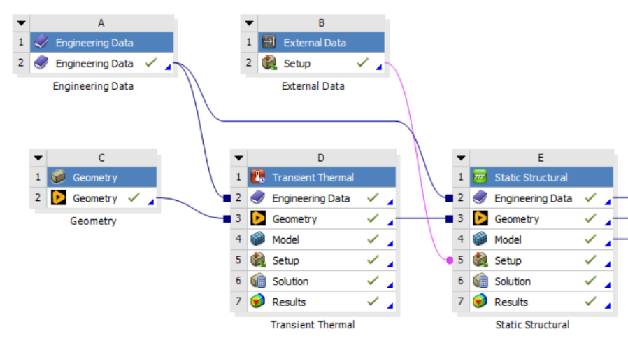
This ME 6124 team project built a representative package model to identify where damage accumulated and to compare design changes that could reduce warpage. A transient thermal solution first captured component-level thermal lag. The resulting spatial temperature field was then transferred into a structural model so the mechanical analysis responded to the actual gradients rather than an assumed uniform package temperature.
Role & Project Scope
The team modeled the package, established temperature-dependent material behavior, designed the thermal cycle, performed convergence studies, transferred thermal fields, and compared the FEA results with reduced-order analytical models. The study was intended to guide package design and modeling choices; it was not a component qualification test or a validated prediction of commercial product life.
- Resolve 10-micrometer intermetallic layers and solder interfaces within a package spanning tens of millimeters
- Capture time- and rate-dependent SAC305 behavior during heating, cooling, and dwell periods
- Separate physical warpage from rigid-body motion without over-constraining the half-symmetry model
- Balance accuracy and available memory after the initial higher-dimensional model proved computationally impractical
Methodology
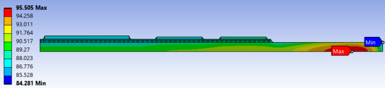
The package was subjected to five 32-minute thermal cycles between 125 °C and −40 °C. Each cycle included 15-minute hot and cold dwells connected by one-minute ramps, for 160 minutes of simulated history. The transient analysis allowed the outer package layers and interior silicon structures to heat and cool at different rates before their nodal temperatures were mapped by coordinate into the structural model.
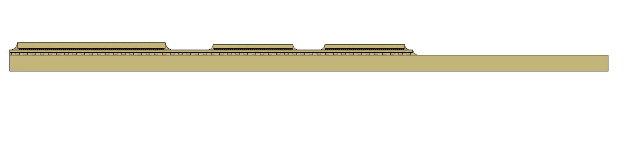
- Built a 2D half-symmetry geometry in Fusion 360 and reused it for both coupled analyses
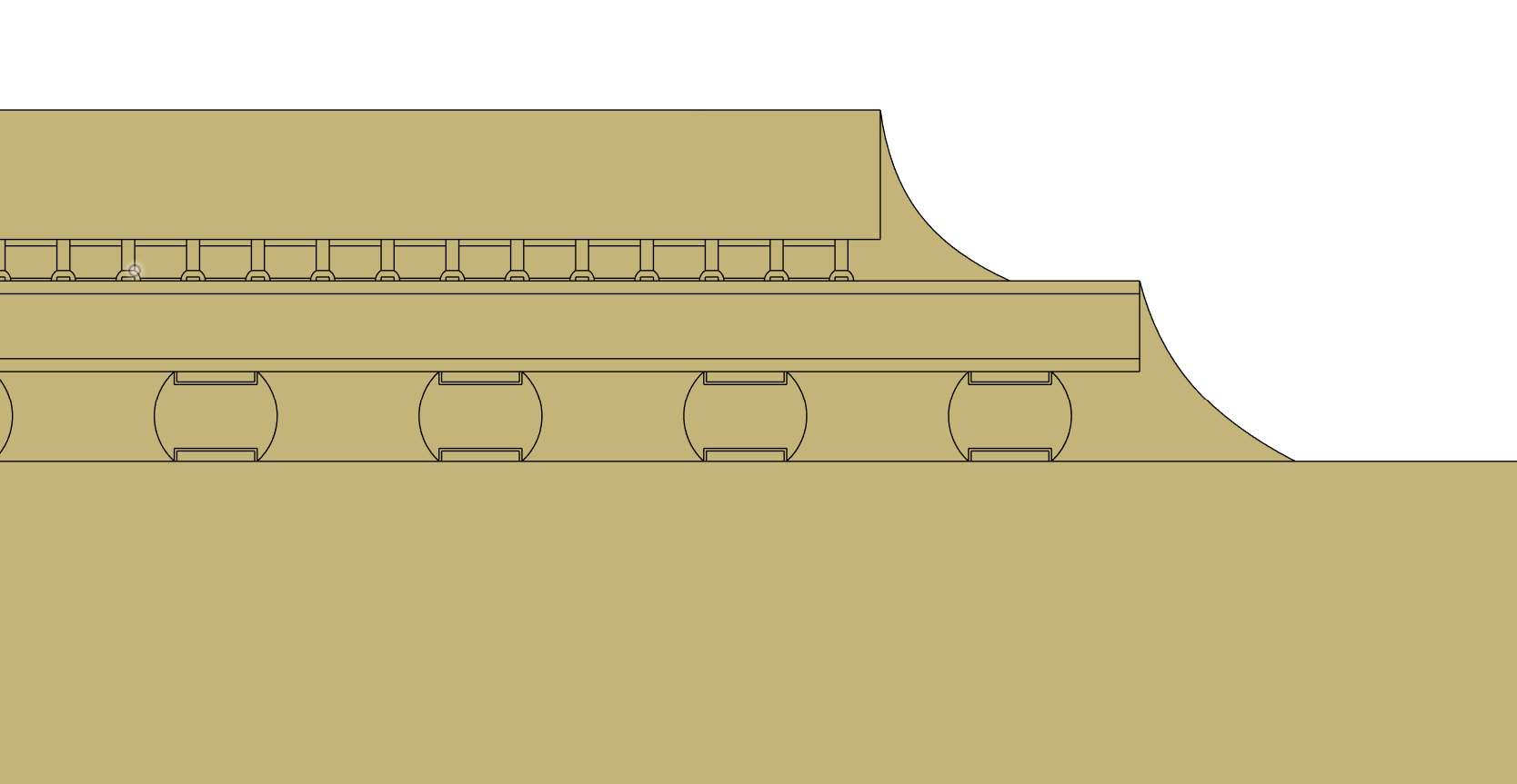
- Generated a 208,948-element mesh with local refinement around solder balls, copper pads, and intermetallic layers
- Modeled SAC305 with the Anand viscoplastic formulation to capture thermal softening, strain-rate sensitivity, and accumulated inelastic deformation
- Applied an anisotropic, temperature-dependent PCB model and copper plasticity instead of treating every layer as a linear isotropic solid
- Selected a 50-micrometer solder mesh after convergence testing from 100 to 5 micrometers
Engineering Decisions & Trade-Offs
The initial 2.5D/full-package concept exceeded available meshing and memory resources. Rather than reducing every mesh region until the interfaces lost meaning, the team moved to a 2D half-symmetry model. This preserved the dominant through-package gradients, solder geometry, and global warpage while making repeated nonlinear thermal cycles solvable on the available hardware.
Mesh density was concentrated where the failure physics lived. Ten-micrometer intermetallic and copper-pad regions received local refinement, while bulk PCB and silicon regions remained coarser. A single-point constraint and symmetry boundary removed rigid-body motion without artificially suppressing the package’s natural bow. These choices were essential: a uniformly fine model was computationally wasteful, while a heavily constrained model could produce visually stable but physically misleading warpage.
Results & Validation
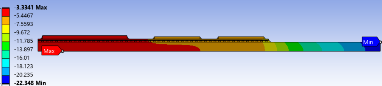
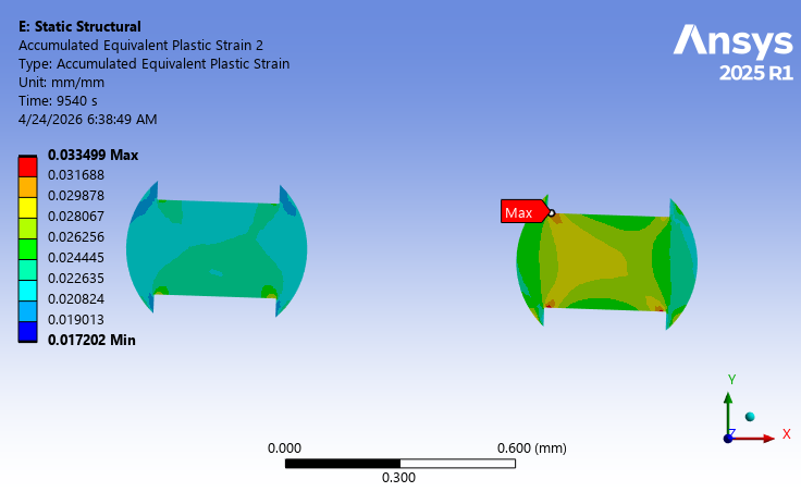
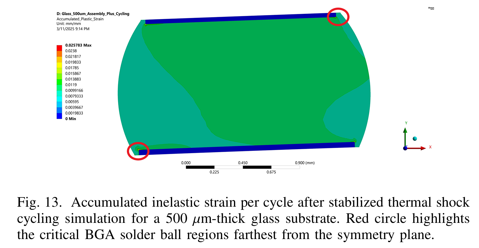
Modeled result After five cycles, the package reached a peak accumulated equivalent plastic strain of 0.0335, concentrated at solder-pad, intermetallic, and copper corners. The localization was physically credible because these interfaces combine sharp stiffness changes, geometric discontinuities, and CTE mismatch.
A lumped thermal-resistance/capacitance model produced a 597-second time constant and a 37.9 °C estimate at 100 seconds, consistent with the finite-element temperature response. Composite-beam theory predicted 2.57 mm of warpage versus approximately 1.8 mm from ANSYS. The difference was expected because the reduced-order model omits solder, copper, underfill, and local geometry, but the comparison established the correct scale and direction of deformation.
Three fatigue relations produced 3,236, 7,084, and 11,506 cycles using the modeled inelastic response. Because those predictions differed substantially from one another and from cited literature, they are treated as an exploratory sensitivity range—not a validated service-life forecast.
Impact, Limitations & Next Steps
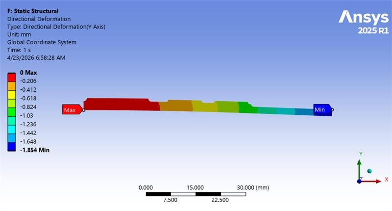
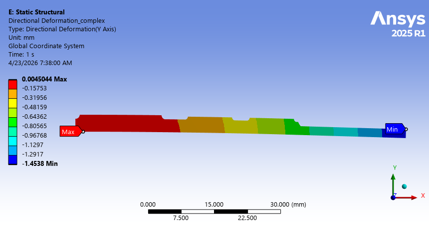
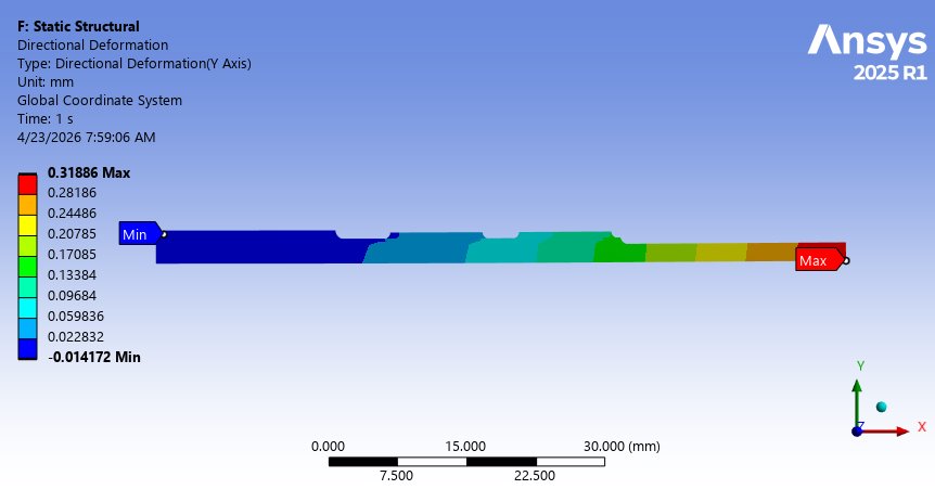
Cooling the package from the 220 °C stress-free fabrication temperature produced approximately 1.854 mm of baseline warpage. Increasing the glass core to 500 micrometers reduced warpage to about 1.4 mm. Matching the PCB and glass coefficients of thermal expansion reduced it much further, to approximately 0.3 mm.
This comparison produced the most actionable engineering result in the study. Increasing core thickness improved bending stiffness, but it did not remove the strain source. CTE alignment attacked the mismatch itself and therefore delivered a much larger reduction. That distinction turns the model from a descriptive stress plot into a design trade study: material compatibility offered more leverage than stiffness alone.
The model demonstrates a credible workflow and useful design direction, but it is not a package qualification result. The two-dimensional representation cannot capture every three-dimensional corner effect, and the accelerated ramps, convection assumptions, and selected material parameters influence the accumulated damage. The fatigue relations require calibration against physical cycling data before they can support a life claim.
A next phase would measure package temperatures and warpage during controlled thermal cycles, refine convection and ramp behavior, and compare solder-joint damage at multiple locations. Those measurements would allow the Anand parameters and fatigue relation to be calibrated while preserving the validated half-symmetry model as an efficient design-screening baseline.